Файл:NE555 Bloc Diagram.svg


Повна роздільність (SVG-файл, номінально 723 × 524 пікселів, розмір файлу: 32 КБ)
| Відомості про цей файл містяться на Вікісховищі — централізованому сховищі вільних файлів мультимедіа для використання у проектах Фонду Вікімедіа. |
Опис файлу
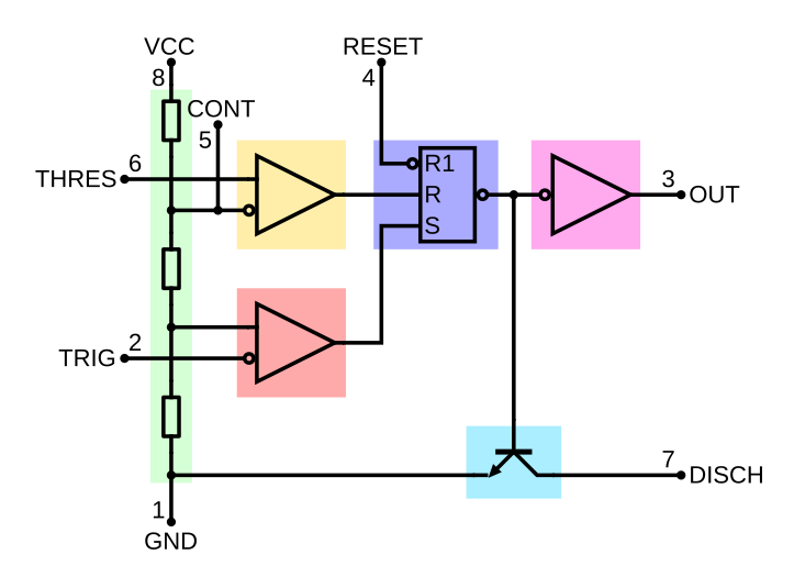
| Опис | English: The NE555 contains 24 bipolar transistors, two diodes and 15 resistors that form six functional blocks: Between the supply voltage VCC (+) and the ground GND (-) is a voltage divider consisting of three identical resistors which, when connected not from the outside, the two reference voltages ¹ / 3 VCC and ² / 3 VCC supplies. The latter is at the terminal pin Control Voltage available. The block diagram and schematic that area is highlighted in green. Two comparators are each connected to one of the reference voltages, while the other two inputs of which are fed directly to the terminals of trigger or threshold. The block diagram in yellow and orange. A flip-flop, deposited in the color purple, stores the state of the timer and is controlled by the two comparators. Via the reset terminal overrides the other two inputs, the flip-flop (and therefore the entire timer device) be reset at any time. At the output of flip-flop followed by an output stage with totem-pole output that can be loaded at the port output with up to 200 mA. Shown in the color pink. Parallel to the output stage of a transistor is connected, the collector is located on the discharge port. The transistor in the circuit diagram is a light blue background, always energized when the output is low level.Deutsch: Der NE555 enthält 24 Bipolartransistoren, zwei Dioden und 15 Widerstände, die zusammen sechs Funktionsblöcke bilden:
|
| Час створення | |
| Джерело | Власна робота |
| Автор | BlanchardJ |
| Інші версії |   |
Ліцензування
| Я, власник авторських прав на цю роботу, передаю роботу в суспільне надбання. Застосовується по всьому світу. У деяких країнах це не може бути юридично можливо, в такому випадку: Я даю кожному право на використання цієї роботи для будь-яких цілей, без будь-яких умов, якщо такі умови не вимагаються за законом. |
Історія файлу
Клацніть на дату/час, щоб переглянути, як тоді виглядав файл.
| Дата/час | Мініатюра | Розмір об'єкта | Користувач | Коментар | |
|---|---|---|---|---|---|
| поточний | 19:54, 16 січня 2012 | | 723 × 524 (32 КБ) | Wdwd | Colored function blocks (for circiut diagram) correct transistor symbol (without a circle, because it's inside the chip) |
| 23:27, 7 червня 2009 |  | 723 × 524 (40 КБ) | Brighterorange | remove spurious red dot | |
| 20:22, 23 вересня 2007 |  | 723 × 524 (40 КБ) | BlanchardJ | {{Information |Description=Bloc diagram of a 555 timer IC |Source=self-made |Date=September 23 2007 |Author=BlanchardJ |Permission= |other_versions= }} {{Created with Inkscape}} {{ElCompLib}} Category:555 timer IC |
Використання файлу
Така сторінка використовує цей файл:
Глобальне використання файлу
Цей файл використовують такі інші вікі:
- Використання в ar.wikipedia.org
- Використання в beta.wikiversity.org
- Використання в ca.wikipedia.org
- Використання в cs.wikipedia.org
- Використання в cs.wikibooks.org
- Використання в de.wikipedia.org
- Використання в en.wikipedia.org
- Використання в es.wikipedia.org
- Використання в et.wikipedia.org
- Використання в fa.wikipedia.org
- Використання в fi.wikipedia.org
- Використання в fr.wikipedia.org
- Використання в fr.wikiversity.org
- Використання в he.wikipedia.org
- Використання в hi.wikipedia.org
- Використання в hu.wikipedia.org
- Використання в id.wikipedia.org
- Використання в it.wikipedia.org
- Використання в ja.wikipedia.org
- Використання в lt.wikipedia.org
- Використання в no.wikipedia.org
- Використання в pl.wikipedia.org
- Використання в pt.wikipedia.org
- Використання в ru.wikipedia.org
- Використання в vi.wikibooks.org
- Використання в zh.wikipedia.org